
More revisions.
I posted the design to /r/PrintedCircuitBoard, and of the comments said:
“Do you need pullups on the outputs of WS2811?”
And of course, I was confident the answer was “no”. For about 5 seconds. And then I measured the WS2811 I have in my breadboard; it gave a nice solid sink when it was on, and when it was off, just a fraction of a volt. Clearly not up to sourcing current to the NPN transistor.
The most likely explanation is that it’s an open collector output:

The collector on the output transistor is just left hanging – it’s only collected to the external pin. The voltage on an open collector can float up above the internal voltage of the IC as long as you don’t exceed the maximum voltage of the transistor
Open collectors are really useful if you want to have a bus architecture with multiple components able to pull the bus low, or if you aren’t sure what voltage of the output is going to be. Since the WS2811 can be used to drive LEDs tied to either 5V or 12V, it makes perfect sense. And it is confirmed by the internets.
Which means that the circuit needs to get a tiny bit more complicated:

Another pullup resistor is added to the mix. Really not a problem from the cost and assembly perspective as the design goes from 9 resistors to 12 resistors.
But, can I fit it in the current board layout without making it bigger?
I should probably add a parenthetical note here that says it’s often easier to go with a bigger layout, and in fact if you are going to hand solder a board, you *should* go with a bigger layout. Though I’m not sure how practical it is to solder the MOSFETS by hand since the base pad is so big…
Anyway, here’s what the board looked like before:
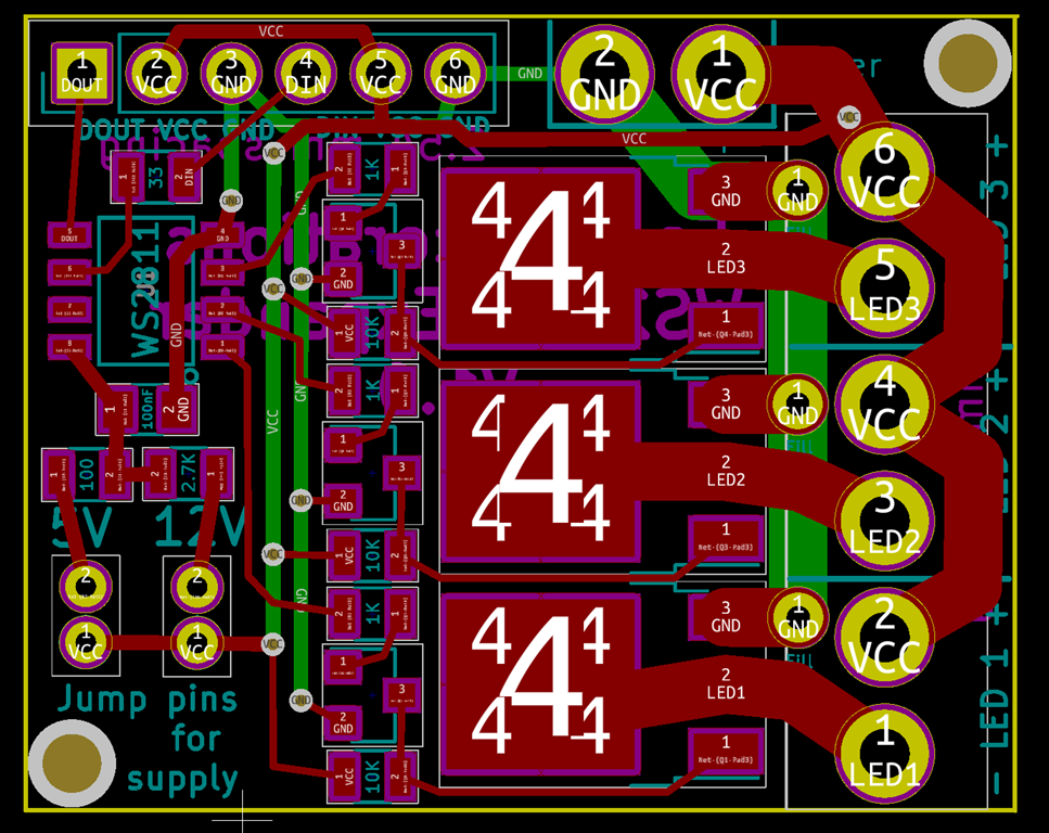
I need to put a resistor between each of the traces that head from the WS2811 over to the transistors. Hmm.
I initially just tried to fit them in there, and with a big of rerouting, I was able to make it fit. Technically.
Then I decided that it would be a lot easier if I moved the vertical ground trace underneath the transistors and used that to provide the ground connection to the transistors. That meant I could move the VCC vias around more easily, and could do the following:

The fit in reasonably well.
I *think* it’s ready to order the first version of the board, but there’s one more step. I now have on hand the WS2811 ICs and both kinds of transistors. So, I printed out a design with the copper layers shown, and did a test to see if the components really fit on the board.

That shows the WS2811 on the left, the MOSFET on the right, one of the NPN transistors and then a tiny 0805 10K resistor at the top. Everything looks like it will fit fine.
I ordered 3 boards for $7.10 from Oshpark, which is my usual supplier for prototype boards if they are small.
So, what do you think ?