For the last 5 years or so, I have led a “Holiday Lights Bike Ride” in early December. It’s fun to tour around and look at lights on a bike, and the view you get on a bike is very different than in a car.
One of the houses has a large snowflake with white and blue lights. Very nice and pretty.
After four years of service, I retired the LED strips I had along my gutters. The “waterproof” strips had started shorting out and it was a pain to replace sections. I personally liked the “line of light” look, but the vast majority of people didn’t even notice that they changed color.
My first thought was to replace them with WS2812 strips, so that I could address all of them. I played around with a few designs, but didn’t solve the design problems to my satisfaction; coming up with a way to keep the strips actually waterproof while still supplying them with power (which you need every 2.5 meters) was a hard problem. So, I put that project on the back burner.
A while back, my Glowforge showed up, and that triggered a new thought about the snowflakes. Instead of doing addressable LEDs on the gutter, could I do snowflakes that hung at gutter level? And then do the gutters with some nice traditional C9 LEDs.
Here are the basic parameters that I came up with.
- Addressable LEDs (probably WS2812s)
- Snowflake outline in acrylic (because I can cut it on my glowforge), white so that the color spreads out, and something like 12″ across (a little small, but it’s an easy size to deal with, and larger sizes make it harder to deal with the wind storms we always get).
- Around 50 LEDs per snowflake
- With local 5V power supply. I’m tired of running 10 gauge cable and worrying about voltage drop, so I want something regulated and local. It will probably be a local 12v to 5v converter, though I might end up with local AC instead.
- Microcontroller controlled. That was obvious with the ws2812 choice.
- *Maybe* WIFI controlled. I’m thinking maybe 8 of the snowflakes, and I can do an ESP8266 across that many relatively cheaply. That would let me drive them in sync from the comfort of my office machine.
The snowflake design was pretty simple; it had to be so that I could easily light it with LEDs.

One of the truisms in these projects is that it’s always the wiring that is the most painful part. That almost killed me on the Snowman project; lots of individual wires, and each has to be cut, stripped, and soldered. Not fun.
I’m thinking about doing 8 of these, so that would be 8 * 50 (leds) * 4 (connections), or something like 800 wires and 1600 solder joints. And to compound that, you need decent sized conductors so that you don’t lose too much voltage along the way.
The way to get rid of all the point-to-point soldering is to use a PC board. Since boards are priced based on their area, I explored using APA102 LEDs which are available in a 2020 package.
That’s 2mm x 2mm, or just a little bit more than 1/16” square. I’m planning on soldering with a heat gun (or maybe I’ll pick up a cheap hot air rework station), but the 2020s will be blown right off the board.
So, it was back to the 5050 (5mm x 5mm) package, and at that point the WS2812B won out on cheapness. The APA102s are nicer but much pricier. Oh, and they have separate clock and data, which is one more wire to try to route correctly.
And there I ran into a problem. A run of eight 12″ x 12″ boards would be right around $200, which is a bit pricier than I had hoped, and it’s not clear to me that I could find a fab that would be able to cut such a fragile arrangement of boards; in fact, I was pretty sure I couldn’t find one.
After some thought, I realized that I could do the snowflake as a series of boards; a central board, 6 straight boards that attach to the central board, and 12 arm boards that radiate from the straight boards.
After a bunch of iterations, it ended up looking like this:

And yes, I did notice the resemblance:

I took that design, pulled it apart, duplicated parts, and came up with this layout:

The PC board will be a little bigger because I’ll need tabs between each part, but it will be close. That is about 5” x 5.3” and has all the parts for a 12” snowflake.
But would it work? Well, a trip to the glowforge with a piece of cheap plexiglass and two minutes of time yielded enough pieces to test it out (the rest didn’t cut cleanly because cheap plexiglass):

The laser loses a bit of material in the kerf, so they are a bit loose, but that will be better with the real design, and it isn’t structural; all of this is supported by the acrylic snowflake, which is thicker and beefier.
It was time to do some board designing. Unfortunately, I don’t have a full license to Eagle, and the free version won’t let me design boards that big (actually looking at the new Autodesk free license, I probably would have been fine), so that meant I had to teach myself KiCAD. Like Eagle, it has a bunch of weird eccentricities which are of course different than the ones Eagle has, and I’ve spent a lot of time researching how to do things that are very simple.
The circuit is really very simple; just power, ground, and a daisy-chained data line. The only big constraints are:
- I want big traces to limit the voltage drop
- I need to be able to connect from one board to another
My usual approach for PC board design is to draw the schematic, and then just start playing around with layout. The layout of LEDs is pre-determined, so it’s really just about routing all the conductors.
Here’s a very ugly schematic:

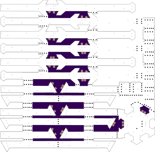
I luckily forgot to save my early versions because they were pretty bad, but with a lot of refinement and rework, here’s version 0.9.

The fat green VCC and GND traces are on the underside of the board, and then the thin red traces (or yellow if there are green lines behind) are the data lines. Wherever there are breaks between the boards, the are solder pads that span across the boards; the idea is that those will be soldered to hold the boards together.
The hub on the right was an interesting challenge; I need to design the pads and place the pads for the other 5 arms so that they will correctly align with the one arm that I did design.
Here’s a close-up of the hub:

The yellow line is the board edge, so what what I have is pads that hang halfway over the board edge and out into space. You will see some small little blue dashes; those are used to align the pads properly on the cutout.
If you look at the little red data line pads, you’ll see that they aren’t so well aligned. I think I’m going to need to redesign those pads with the same alignment marks so they can be better aligned. Then I’ll have to tear out most of the data lines and the old pads, rotate each new pad to the proper angle (each one is different because of the shape of the recess), and then redo all the tracks that run to them.
Such is the nature of PC board design; you think you are done, and then you need to do a bunch of re-routing.
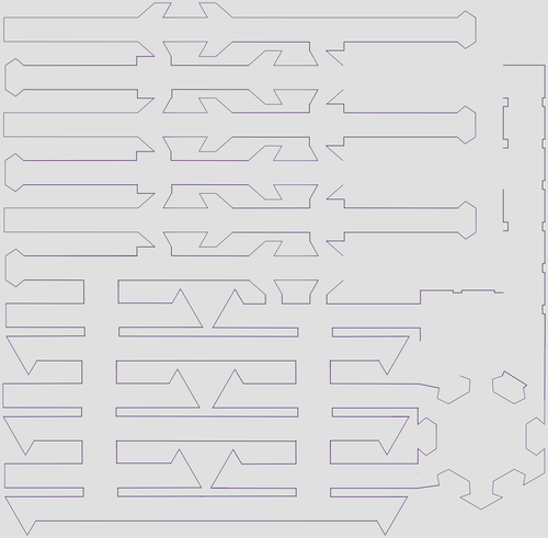
Luckily, the tool helps out a lot; the system knows which pins should be connected to other ones. If I get rid of some of the connections, it looks like this:

Each of those thin gray lines shows a connection that is made in the schematic, but is not correctly made on the board. The software also has a number of other design rules that help you find mistakes.
At this point, I upload is to OshPark, which I like for small boards, and it gave me this as a final design view:
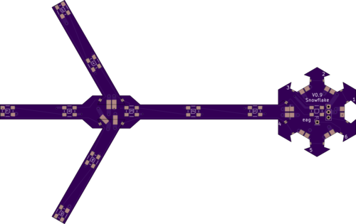
Which looks pretty nice. 9 LEDs on each arm plus one on the hub gives me 55 LEDs per snowflake.
Given the size of the scrunched together version, I think I can get the boards for 8 full snowflakes made and delivered in 12 days for around $80, which is pretty good.
The downside of this approach is that you spend a lot of time on the pc design, but I’d rather be doing that then spending days straining my eyes and back hand-soldering.
Now the big question is, “how lucky do I feel?” Do I order a whole run at once, or do I order one and verify that it works before ordering the other 7?