
I thought that I was done with the PCB design, but it turns out that I wasn’t close.
Basically, I ran into two big issues.
The first was the wierd angles that I had in my design; they didn’t pack together very well. What I really needed was a way to rotate the two short arms so they were at 90 degree angles.
I couldn’t find anything, so I went and wrote a utility to do it. On the way, I learned a lot about the KiCAD file format. It was a nice little exercise; I’ll note that it’s in pretty rough shape and you would need to recompile it to get the rotation you wanted (and to work on the file you wanted); maybe I will clean it up at some point. It’s C# code because that’s what I speak best.
I guess I should also note that I built a little .pcbnew parser to do it; it parses the file into a bunch of nodes, you change the ones you want to change, and then it writes the file back out the way it was before except for the changes. So, it will likely be useful for other stuff as well.
So, anyway, that gave me everything at increments of 90 degrees, which was good. Then I went off and started trying to understand if PC fab houses could build what I wanted. The answer seemed to be “yes” (though not in the current form), but they would likely charge extra and there was a decent chance they would make a mistake. The problem is that I have 4 different irregularly-shaped boards. You can’t use v-groove panelization because that only works with (mostly) rectangular boards. I was hoping to use the GerberPanelizer, but I couldn’t get any of my boards to show up in it; I suspect it’s because of their shape.
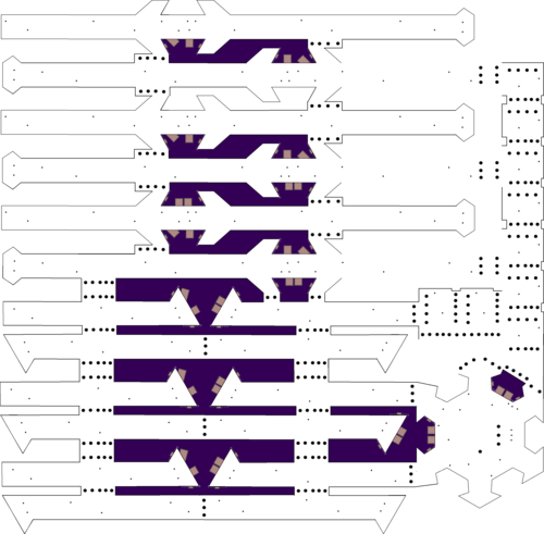
So, I went off and taught myself the requirements and spent a bunch of time coming up with this:

This is a hand-panelization of my boards. The idea is to come up with a design that can be fabricated as a single piece by the fab (and assembled/soldered/etc., if you are planning on having somebody do that) but can still be easily separated.
You do this by putting little breakaway tabs with small holes (I used large vias because KiCAD only supports holes in footprints). The idea is that after you get the pcb, you can carefully break off the parts with the weak tabs to separate the boards. The tabs are also called “mousebites”.
To make them breakable, you need to design things so that you have multiple tabs that are in a line and could easily bend. That isn’t even close to possible with this design, so what I’m going to do is cut the boards apart with my Dremel rotary tool or oscillating multitool. The rough edges will not matter for this application. If the design is correct, all the yellow edges will be cut with a router after the PCB is etched.
Oh, and the small boards on the right are little WS2812 breakout boards; I had a bunch of extra space in the square, so I added them in.
My first check is to upload to OSHPark and see what it thinks; I’m not going to order there but it does full visualization of the boards. Here’s what I got for the board and the board outlines:
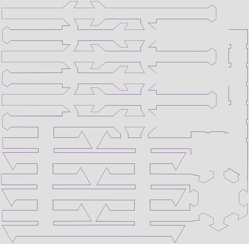
Yeah, that’s not very good. The design looks fine. However, when I was switching between layers, I accidently chose the “Eco2.user” layer instead of the “Edge.Cuts” layer. They are rendered in the same color. All I needed to do was to turn off that layer, and then I could flip those lines over to the edge cuts layer, and that fixed the issue.
OSHPark still has trouble with the design, but I’ve exported Gerber files (one file per layer in the design tool) and looked at them in other viewers and they are fine. I think the OSHPark viewer is having trouble with the internal cutouts.
Because of the complexity of the design, I’m not sure how to spec it on the online ordering tools, so it is currently out to order.
So, what do you think ?