My original plan for the controller was to do all the wiring by hand on a perfboard (“old school”); it’s not that complicated and I wouldn’t need to wait for a board. But I decided to do a pcb board to see how much it would cost and because I wanted an excuse to try out Kicad 5.0.
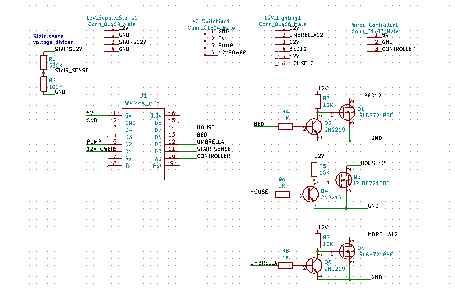
I started with the schematic:
We have the Wemos D1 mini (clone, actually) in the middle, with 5 outputs (PUMP, 12VPOWER, HOUSE, BED, AND UMBRELLA), and two inputs (STAIR_SENSE and controller). If you haven’t seen labels used in a schematic before, every pin with the same name is logically connected though there is no wire drawn between them.
On the right we have three drivers for the landscape lights using the NPN transisitor/MOSFET circuit I discussed in the last post. All of those outputs connect to the 6-connector header (screw terminal) strip.
On the upper right, the Wired_Controller1 header will be for a (possible) hard-wired controller for the lights and pump. It’s connected into the analog input of the ESP. In the actual handheld controller there will be four switches hooked across a voltage divider so that the switches will give 1V, 0.75V, 0.50V, or 0.25V when pressed. The ESP code will figure out which switch was pressed and therefore which action to take.
In the middle is the AC_Switching1 header. It contains the two outputs to control the remote solid-state relays for the pump and 12V power supply. It also contains the 5V and ground from the 5V power supply that will run the ESP.
On the left we have the parts for the stair light sensor. We have a voltage divider that will convert from the 12 V that will come in to a value that the ESP can tolerate. There was a bit of calculation there. The valid ESP8266 input voltages range from 2.5V (for the lowest guaranteed high value) to 3.6V (the maximum input without damage). We want to choose the voltage divider ratio to work well within that range.
My first choice was to use 330K for the upper resistor and 110K for the lower one; that would give a 4:1 ratio. That would put the lowest guaranteed high value at 2.5*4 = 10V, and the highest tolerable value at 3.6*4=14.4V. I decided I wanted a bit more range on the high side, so I opted from 330K and 100K resistors, giving a 4.3:1 ratio, and a voltage range of 10.75V to 15.5V. I considered overvoltage protection, but given the ampacity of the supply a simple zener likely wouldn’t be enough and I would need an SCR crowbar to handle overvoltage. I decided to skip it in this version as the power supply is a regulated one.
That’s all for the schematic; not really that sophisticated. Oh, the NPNs are really 2N2222; I chose the 2N2219 because it already existed.
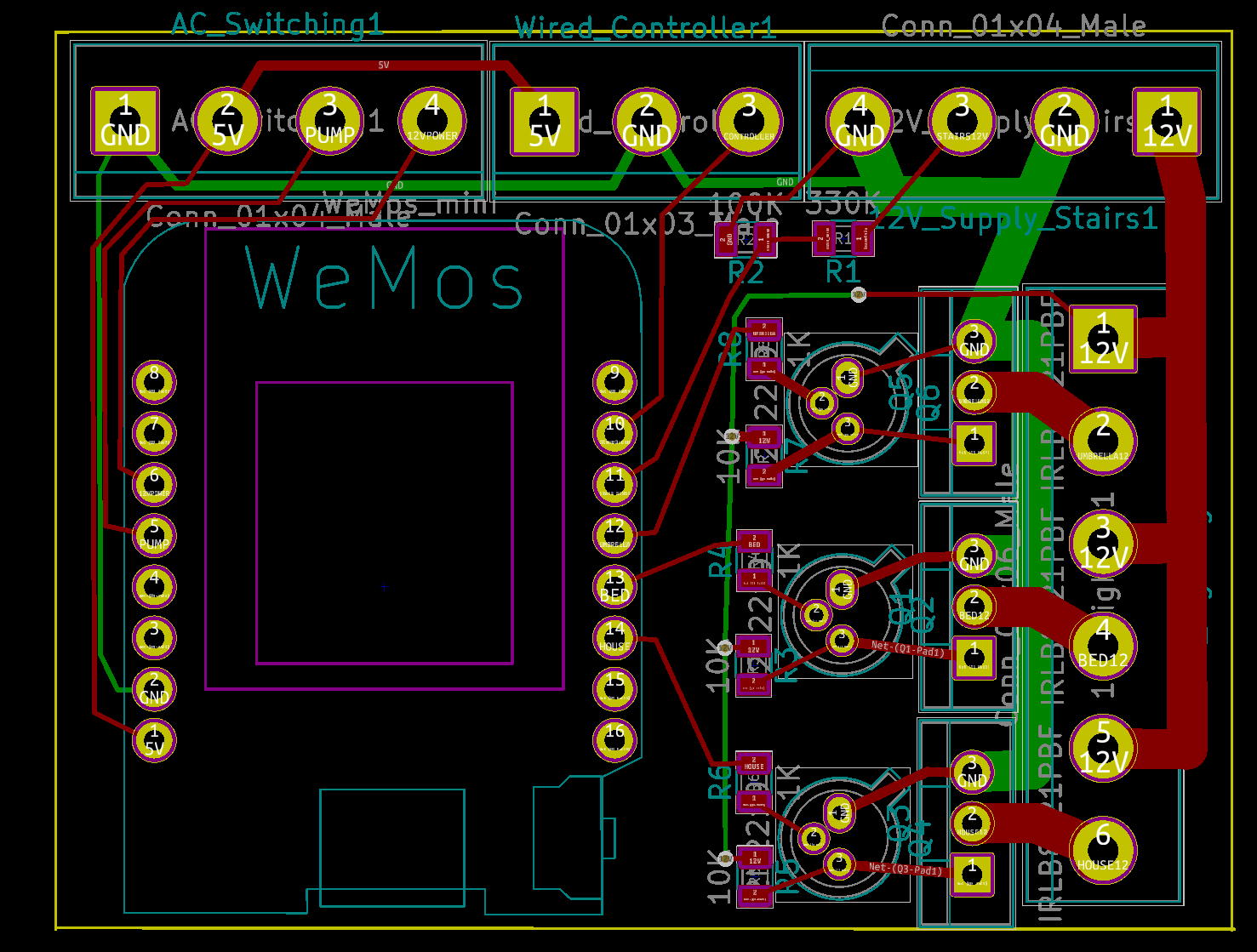
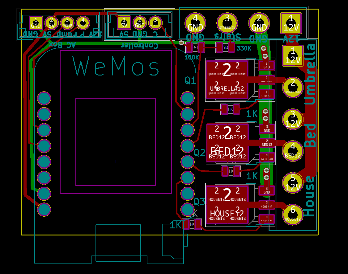
Here’s the board layout. It’s a weird mix of through-hole and SMD components as I already had both the MOSFETS and the NPN transistors. I started with the header for the landscape lights because they will be pulling some hefty current; that meant I wanted to keep the traces short, and it also meant that I wanted to put the 12V in nearby in the upper right. The controlled where the MOSFETS ended up, which controlled where the NPN transistors and their resistors ended up. I reordered the output pins on the header so that they matched the order of the output pins on the ESP module; I could have remapped the pins as well but this was a bit simpler. The AC switching header also got re-ordered to make the connections simpler. And then I tightened things up a bit to minimize the size of the board. At that point, it was about $20 to do a board from oshpark, which was pretty much the cheapest I could find.
That’s relatively cheap, but I’m not excited about having to wait for it to make it back to me. The footprints for the screw terminals is not based on a header that I have; I bought some terminal strips before I decided to do a board design, but I need to buy some better ones for this sort of design. I need to get real terminals so I can get real dimensions, and I might see what I can do with all SMD devices; smaller terminals and transistors could cut the size of the board by 25%.
Two more things to mention. You’ll notice that there is not a copper pour for the ground. It’s probably not required for a board operating at these speeds, and I would have to be careful around the ESP8266 antenna because having copper underneath it would mess it up.
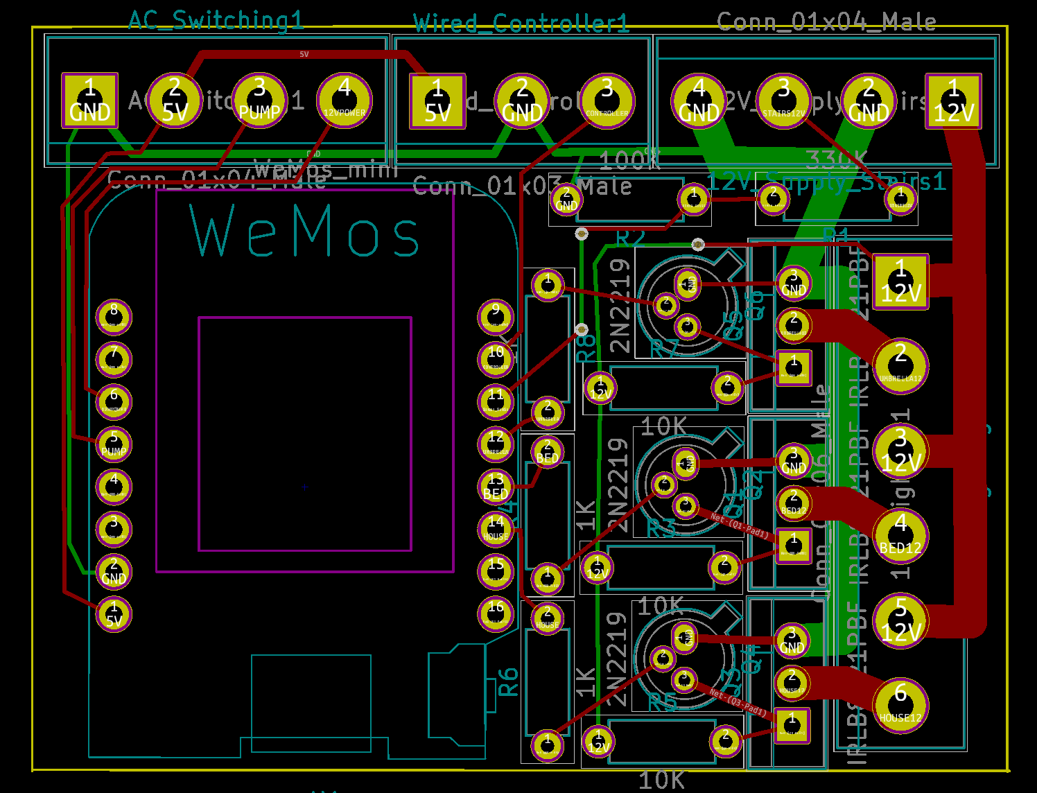
I did another layout with through-hole resistors in case I wanted to hand build it:
Back to the problem in hand… If I was willing to wait for a PCB to show up, I could wait for some new MOSFETS and transistors, and that would certainly make things smaller. So, I went MOSFET hunting, and I found the IRLR7821PbF, available in a TO-252AA package at $6 for 5 MOSFETS. Sound good.
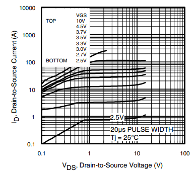
I pulled up the datasheet and started reading. It’s pretty similar to the IRLB8721 that I had currently specified, but on Page 2 I found the output characteristics graph:
Looks like the one we saw in the last post, right? Except this this one starts at 2.5V and 2.7V curves. Looking at the 3.0V curve – to be conservative – and we see that with 10V drain to source, we can get a little more than 10 amps of current at a junction temperature of 25 degrees. At 3.3 volts, it’s closer to 12 amps.
What that means is that we can drive this MOSFET directly from the ESP8266. We can lose the NPN transistors to drive the MOSFETs plus one of the resistors.
So, off to do a new design with this MOSFET. I decided that I’m going to mount the board, run wires from the board to some terminal strips that I have, and then hook the real wires to those terminal strips. That will make it easier to hook up and I can make the board smaller so that it will be cheaper.
After a lot of iteration, here’s what I end up with:
It’s about 30% smaller than the original board; part of that is done by letting the ESP board overhang the end of this board, but they will both be in an enclosure (3D printed, I think), so there’s no harm in that. All of the heavy current stuff is contained on the right side of the board.
I first head to OSHPark, which tells me the board is 48mm x 37mm. That’s less than half the size of a credit card, so, tiny. They will make me 3 boards for $13.30, and oshpark does really nice boards, with an ENIG finish, but they take a couple of weeks to show up. I head next to pcbshopper.com and find nobody cheaper, except allpcb.com. I used them for the boards in my dodecahedron and they’ve done good work, and I can get 5 boards in 5 days for $10, shipping included. They must be blackmailing DHL to be able to ship so cheaply.
I’m trending towards OSHPark since I need to order the new MOSFETs in anyway.

So, what do you think ?